
|
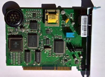
US Robotics Sportster 33.6 #840 modem (V.34) - Late 1996 You now have the ITU dialup handshake tones (or "that abominable screech") in your head. The initial buzzing noise was frequency shift keying (FSK) data where the modems started out at V.8bis, upgraded to full V.8, disabled the echo suppressors on PSTN (or tried to), then told each other what they could do. Just after that, and before data began, a high pitched series of tones measured the telephone line and then agreed on a working symbol rate. They then trained against each other and began proper user-data transmission. The speaker is muted at that point. Back in the day, there was a big thing about "real hardware modems" against "Winmodems". Winmodems implemented the DSP in software, and the modem itself was just a digital to analog converter and a telephone line interface. Hardware modems did not, they ran off a serial interface (or a fake one over a PCI or ISA slot) and handled all the data compression and encoding themselves. In the late 486 and early Pentium days, a Winmodem could substantially hit the CPU. By the time CPUs reached 200 MHz and beyond, it was a non-issue. This one, like quite a bit more around here, came via Bryan McIntosh: It's a US Robotics Sportster 33.6K modem, which I received as a birthday present from my parents in January of 1997. It was supposed to be my gateway to the Internet even though I was using a crusty 386 DX-25 at the time with Windows 3.11. We never ended up actually connecting the modem to anything since my parents (wisely) insisted that we get a second phone line before I started inevitably tying it up while surfing the mid-90s web; we got the second phone line in the Fall of 1998 around the same time that I got a shiny new PII-300, my first modern computer (more hardware from that box to come when I get around to taking pics), and this Sportster just sat inside the 386's case waiting to be used.A look around USR's legacy site finds how we can work out what model we have: It's the SKU 000840-03, identifying it as a Sportster 33.6 #840. Of course this doesn't much help, as there were eight versions of the 840, some compatible, some not. Had we blown the $60 for the X2 upgrade in 1997 or so, USR would have sent out a PLCC chip removal tool and a new PLCC chip to fit on the modem. This would have got a maximum sync rate of 53,333 bps (in real life, this would have been between 40K and 47K). Rockwell sponsored the K56Flex standard, while USR developed the X2 standard, neither of which were open standards, and neither compatible with the other. In general, K56Flex saw more support due to ISP equipment more easily being upgradable to the K56Flex standard: Rockwell made nearly 80% of all ISP modem equipment. US Robotics was a well regarded vendor, and this is a well implemented device. We'll have a vaguely clockwise tour of the PCB, starting at the upper left. That big round thing with the holes in it is a speaker! It's responsible for the modem handshake and training sound. Moving on is a little 28 pin PLCC package, labelled TLC 320AC01C-FN, an analog interface. Today we'd call it a codec, as it is integrated full-duplex ADC and DAC. It has an internal low-pass filter which cuts at 3.6 kHz. It feeds the speaker, via either the op-amp just above it or the one just below the speaker, but is primarily responsible for interfacing with the telephone line. The signal going into the analog interface goes via the big yellow thing, a 1:1 isolation transformer. The beige/brown/orange thing is a metal-oxide varistor, which protects against line surges. It lacks a ring capacitor, which regenerates the ring signal on a phone line chain, so the device along in the chain, if an old analogue phone, would not ring (these were extremely rare by the time of modems). The blue thing beneath it is a relay. This "picks up" the line. Being 8-bit ISA, this guy needs jumper configuration, and the jumper block allows us to configure which COM port and which IRQ the device will be configured to use. It can use IRQ 2, 3, 4, 5 or 7. Just to the left of this is the TL16CFM504APJM controller, which is a member of the TL16C ISA controller family. They are dual UARTs with 16-byte FIFO buffers. This handles the ISA bus and acts as the first stage of an ISA to RS-232 converter. Just next to it is a National Semi 74VHCU04 hex inverter (six NOT gates) just above a 4.281 MHz resonator (an oscillator has four legs, a resonator has two) which isn't a standard or common frequency. Moving along, the 80 pin PLCC is a TI PD17804PJ CDSP (custom DSP) which is linked to the two chips below it (they're in parallel), which come later. The 80 pin package is the main modem DSP. The two identical chips below it are SRAMs manufactured by ISSI: The IS61C256AH is a 32,768 word, 8 bit CMOS static-RAM, so 256 kbit or 32 kByte. These have date code week 37, 1996 and, together, they give a 16 bit 64 kB SRAM capacity, used by the DSP for workspace ("scratch"), buffering, etc. Finally, the Atmel AT27C2048 (date code week 41 1996) is a 128Kx16 (2,097,152 bits) OTP EPROM, programmable at 12.7V but only one-time programmable. Faint markings of perhaps a sticker can be seen on the EPROM, which appears to be a copyright notice and a date. The replacement, for X2 operation, had a fancy X2 logo on it, so we know this one wasn't upgraded. |
|
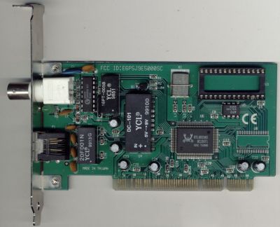
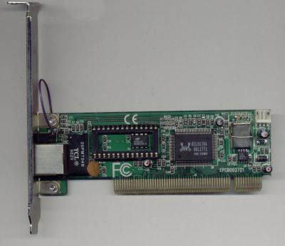
Realtek RTL8029AS ISA ethernet network adapters were usually BNC and later RJ45 for 10BaseT, which rapidly emerged as the dominant medium. It was, however, quite rare to see 10BaseT in both BNC and RJ45 forms on a PCI card, this arrangement normally reserved for their elderly ISA brethren. The RTL8029 was one of the few 10 megabit adapters with PCI compatibility, and also supported 10Base2, 10Base5, however neither could handle hot-plugging the network cable. As this was at the end of 10BaseT's life, there were many features on-die. It could program a 9346 EEPROM without any assistance to use as boot-ROM. Like most of the day, it was NE2000 compatible, like this really meant anything, it could work in a Novell Netware environment. The Novell NE2000 was Novell's way of selling more Netware licences. It was a crude National Semiconductor prototype (8390), but Novell could not sell much Netware since IBM and 3Com charged an absolute fortune for networking hardware. Novell decided to produce a reference design around National's 8390, the NE1000, for $495 USD in 1987. This undercut 3Com by about 50%. There was no royalty needed for compatible designs, and Novell allowed its distributers to go direct to the manufacturer. AMD's (buggier than an ant farm) LANCE-7990 was a significant competitor. This RTL8029AS was originally intended for Cat-3 cable, as can be seen in that only two pairs are used, it wasn't until Cat-5 that four pairs of conductors were used. UTP cable allowed full duplex operation, and although the RTL8029 wasn't great at it, at least traffic in one direction did not cripple traffic in the other. The 8029AS was basically an 8019AS with a PCI interface. |
|
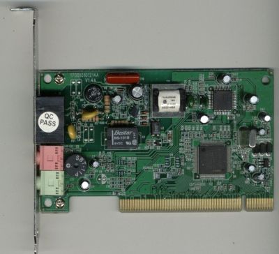
Intel 536EP 56k PCI Modem Intel had long believed in using the power of their CPUs wherever possible and their modems were no exception. The 536EP was a development of Ambient's PCI softmodems, after Ambient had been bought by Intel. The main DSP was implemented in hardware, but the error correction and compression was done in software, making it a hybrid of hardware and software, not a true hardware modem and not a true software modem. As we can see, this uses an isolating transformer between the digital and analog sides of the modem, it was before silicon DAA isolators were common, though it does have a pair of MOVs (the gold coloured components near the line sockets) to protect against transients. |
|
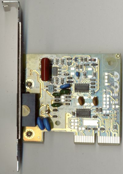
Holy Crap, It's an AMR card! AMR slots were the Intel version of the more open CNR riser and were exactly the same thing. They appeared on quite a few motherboards but it was exceptionally rare to find them in use and the cards themselves could be bought from virtually nowhere. They are simply the analog side of a dialup modem, the digital side done in the MC'97 southbridge and on the host CPU. In this one, like all dialup modems, the blue components you see are metal oxide varistors (MOVs) which are commonly used for surge protection, the big brown thing is a non-polar high voltage capacitor (250V rating) used to regenerate the ring line on a UK (BT) line, where the ringer can be regenerated - this modem had a line pass-through. As the ring line is a third line and RJ11 carries only two conductors, it is regenerated on each device. The upper IC is a (PCTel) PCT303W DAA (data access arrangement) phone-line interface providing isolation and the lower is a Silicon Laboratories Si3024-XS8 DAA which interfaces with the MC'97 southbridge and converts the MC'97 serial audio data back into analog audio for either voice or data use. A similar pair of DAA chips in 16 pin SOIC packages can be seen on most modems, common pairs are the PCT303W/PCT303D and Si3012/Si3024 (collectively known as the Si3036 - datasheet). Modems without DAA ICs have to use isolating transformers and seldom come with MOVs. |
|
Realtek RTL8139A A cheap, no-nonsense NIC bought in late 1999 and still in daily use in 2007. This particular specimen cannot run reliably above a 35MHz PCI bus, so facilitated zero FSB overclocking. For that reason, it was demoted to the dual system which can keep its PCI bus in spec at its normal working frequency. The activity LED was once cut out and the wire soldered on to work a front panel LED. Sadly, the network it was on at the time was hub based and not switch based, so the LED was always flashing. The RTL8139 itself was never a great performer, being about as basic as a NIC could get in terms of function, so needing the host CPU to handle pretty much everything. However, the RTL8139 was cheap and very reliable so it made design wins across all the top-tier OEMs; An 8139 just works without needing external drivers on everything since Windows2000 and up. Many techs carried 8139s in their toolkit, such is the importance of network connectivity and if the card got broken it was cheap and easy to replace it. The "A" variant denoted it had Wake-on-LAN functionality via "magic packet" or "wakeup frame", but it needed an extra cable to the motherboard to enable this. It needed split signal for the clock, 25 MHz and 50 MHz. This was handled by the 50 MHz oscillator (position X1) and the small 8-pin package beneath it. |
|
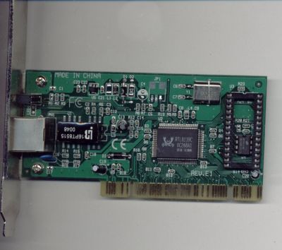
Realtek RTL8139C This one is similar to the above, but on a larger PCB and using a later revision of the 8139 controller. It can handle an overclocked PCI bus up to 44MHz. Neither of the two Realtek NICs are great performers but they can push 80Mbps when asked to. The "C" version is made for 3.3V operation and has ACPI compliance to PCI 2.2 specification, so does not need a WOL cable for Wake-On-LAN. It includes the "B" variant's ability to work from a small 25 MHz crystal oscillator (position Y1). The "D" revision (not terribly common) re-adds 5V compatibility. |
|
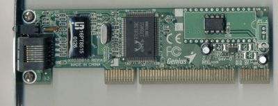
Realtek RTL8139C Genius are known for end-consumer marketed upgrades (usually keyboards, webcams and mice), which means their quality somewhat sucks and their price tends to be high; but the box and packaging tends to be flashy. This is about as cheap and trashy as an 8139C could ever be. This card cost twice as much as the one above, even though it's obviously cheaper to manufacture and was three years later. It never performed reliably (which was incredible for an 8139) and eventually was retired from service to be replaced by a Netgear. |
|
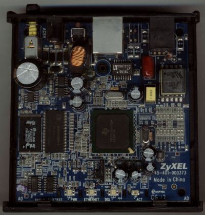
ZyXEL Prestige P660R-61C Well built to good quality standards, ZyXEL make good workhorse SOHO network products. It is based around the Texas Instruments AR7 single chip DSL modem/router using the 7300A chip. The firmware is stored on Intel flash memory (2MB capacity) and no custom firmwares are available due to ZyXEL's habit of using specially modified bootloaders and a custom OS, ZynOS. The 2MB capacity somewhat puts a damper on things too. The router does not have the ability to set target SNR and, indeed, most commands on the CLI are locked out and do nothing. DMT5.22 will work with this router, but little else will. UPnP is supported but with UPnP enabled most games will suffer great lag until the router is rebooted. Running BitTorrent clients seems to cause this and, regardless of whether the client is still running or not, only rebooting the router will solve anything. It's cheap, it's well built, it's easy to configure and use, it usually just works without issue, but it's not for the advanced user or anyone who wants to be hacking firmwares. |
|
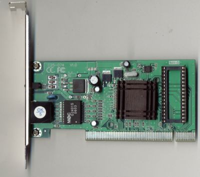
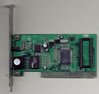
Realtek RTL8169S I couldn't get the heatsink off without potentially damaging the card, so it remains unidentified. There's no UL or FCC number on it and the only identifying mark on the back is a barcode sticker with "NC-1000TX-R06030973" printed on. My best guess from the size of the IC and layout of the card is some variety of Realtek, possibly an RTL8169 or RTL8110. As it has a heatsink, it's pretty early, so I'll tip it to be an RTL8110. A single port PCI NIC with a heatsink, whatever next? With the heatsink finally off, the chip is clearly seen to be an RTL8169S, one of Realtek's first ventures into gigabit ethernet. Due to the complex DSP required to operate on upwards of 100MB/s (not that PCI can sustain that), these first generation models all required small passive heatsinks. Judging by its peers, this heatsink is smaller than the others, so may well be the cause of its slight instability. Update - It's been put into use and identifies with a vendor ID of 10EC, which is Realtek, and a product ID of 8169, which likely puts it in the 8169/8110 (MAC/PHY) family. However we need to be cautious about a firm identification. While they're largely software compatible they do differ in their product IDs. Realtek have long used sensible numbers in the PCI ID codes, So an 8167/8110 will identify as "8167". They use an identical driver, right down to the same files, and appear identically in Task Manager. This card doesn't have J1 (WOL connector) fitted and it knows it; Properties page in Task Manager omits the Power Management tab. |
| [Not Yet] |
Realtek RTL8168/RTL8111 I just wanted this here as a note. The RTL8168 MAC and RTL8111 PHY are common basic Ethernet components (and usually integrated on one chip) used on many motherboards and are a PCIe version of the 8169 (just above). All variants of this cannot do jumbo frames reliably. The driver exposes 4K and 9K frames but you will see extremely poor throughput or even complete failure. This whole line of components is broken in Windows and Linux when doing jumbo frames, it is best to simply disable that feature. |
|
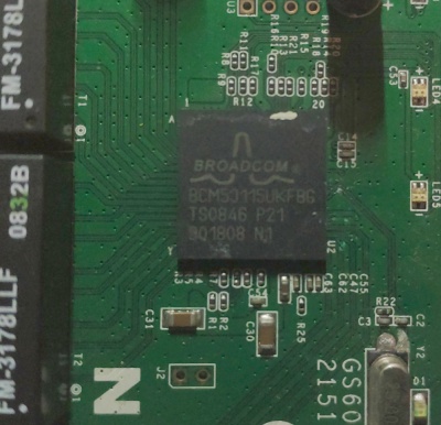
Broadcom BCM53115U Sometimes very influential and important hardware goes completely unsung. To understand the importance of the BCM53115, we must understand its context. From around 2005 onward, low cost network adapters started to spring Gigabit-Ethernet 1000BASE-T (GigE) capability. By 2010, they were ubiquitous, but the fabric needed to handle GigE was not so much. A four port unmanaged gigabit mini-switch was around £70 when the PCI or PCI Express card with a port was dropping below £20. Five years earlier, and the Intel PRO/1000 GT could cost the same as an entry level laptop. Gigabit had a lot to offer to home user who may not have had a special crossover cable needed for nearly all Fast Ethernet (100BASE-T) port-to-port as it had Automatic MDI/MDI-X Configuration, it could detect if it needed to crossover or not. Uplink ports, selection switches and special-purpose cables were obsolete overnight and most engineers would say "good riddance". 1000BASE-T used the same category-5 cable (Cat-5e and Cat-6 were compatible but unnecessary) out to the same 100 metre range as previous Fast Ethernet and was really a drop-in replacement. Until around 2010, however, it was just too expensive to be used. Enter BCM53115 in mid-2009. With five non-blocking PHYs and two uplink RGMII/GMII/MII interfaces, it was suitable for smart switches, routers, and gateways, but also the the uplinks (one for a CPU/SoC, one for a WAN connection) could be completely ignored and the chip used alone as an unmanaged switch. Alternatively, it could provide backhaul for WLAN, router, etc. devices, as it was capable of managed operation with at least one of the uplink ports connected to a processor. Broadcom made three variants of the 53115, the M, S and U. M was full featured and intended where 802.1q, VLAN and QoS were important, such as gateways and routers. S disabled CFP and QoS, U disabled the two uplink ports and everything but for layer-2 switching. This variant is the 53115U, intended for unmanaged switches, and this is exactly where we see it, in the Netgear GS604 v3. The switch adds power supply, decoupling and passive components, and a 25 MHz oscillator. Component count was minimum, PCB size minimum, power was specified at 12V 1A. 12 watts of power in such a small space and on a BGA chip with a sintered alumina ceramic plate stuck to it as a heatsink would be unwise, and this is really only there in case all five ports are taken to the maximum cable length they are specified for, 100 metres, so needing the highest transmission power. This can, in theory, peak at 15 watts, but never sustain more than around 9 watts. BCM53115, built on TSMC's 65 nm process, was a game-changer for gigabit ethernet. Gigabit then became ubiquitous as this chip, and those like it, found design wins across the board. By 2015, low cost ADSL/VDSL/Cable routers were gigabit based and only the very, very low end of things (e.g. Asus DSL-N16 xDSL modem-router and its ilk) were stuck on 100 Mbps. |
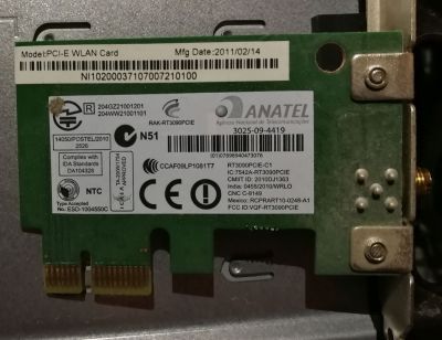
|
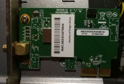
Anatel RT3090 PCIe WiFi Card This little guy lived in an extremely unlovely Packard Bell imedia S1800, manufactured March 2011. The date of manufacture on this card is Feb 14th 2011, the HDD (A 7,200 RPM 1 TB Hitachi, probably the best component in there) was October 2010. A Valentine's Day WiFi card, is there anything to love about it? No. No there is not. It uses the entirely basic Ralink RT3090 chipset, supports the usual 802.11b/g/n (initial certification was draft-N), doesn't support the 5.2 GHz band, doesn't support MIMO and so can peak at just one spatial stream of 40 MHz, so a peak symbol rate of 150 Mbps. This would translate to a data rate of about 80 Mbps. It wasn't even any good for the time, it was the most basic thing able to add "WiFi" to the spec list. Thr RT3090 did support antenna diversity (two antennae) but only in so much as switching between them for the best signal, it wasn't in any way able to do MIMO. Either way, the second antenna feed is not fitted at all on this card. It isn't even an unfitted option on the PCB! The design is our next clue. This cut every corner possible, then more. Usually, a desktop WiFi adapter would be a mini-PCIe thing intended for laptops, placed on a PCIe x1 slot adapter. This, if you're wanting decent WiFi, is the most cost effective, as mini-PCIe cards are made in immense bulk and the adapter is no more than a mounting and the fitting for the port. Dell does this across its entire range. However, if you're a decently sized OEM, like Packard Bell, you can specify whatever you want to keep costs down, if you're ordering enough of them. If you're cutting costs everywhere else (the sole video output on this system was VGA, when VGA was obsolete already!), half a buck on the WiFi card soon adds up. Crummy card from a crummy PC, but installs out of the box on Windows 7 and up. |
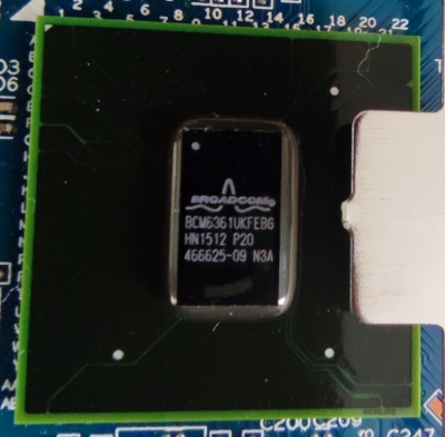
|
Broadcom BCM6361 - 2011 This early-2010s home/small office (SOHO) networking all-in-one was seen in quite a few designs, this one being in Netgear's D6200. In the D6200, the BCM6361 was a little outdated (as seen in the really dated UI it used) so Netgear added a BCM4352 mini-PCIe card for 802.11ac. No, an actual, recoverable, reusable, mini-PCIe card just like in a laptop! The spec of the SoC was two BMIPS4350 cores at 400 MHz, hardware assist for bridging and routing, hardware crypto for IPSec, a 2x2:2 802.11n on 2.4 GHz and 5 GHz via integrated BCM2057r8, four 10/100 Ethernet PHYs and dual GMII interfaces, which go via switched PHYs to four gigabit ethernet ports. It also has a USB2.0 host and device capability. The BCM6862 adds DECT ability. Importantly for a UK/EU-market solution, it had a built in ADSL2+ modem with its own MIPS32 core to handle ATM processing. For 2014, this was a decent level of performance, you'd expect to pick one up for around £130 in the UK. 802.11ac was new and cool, but the implementation was sorely lacking. The WiFi for this unit was widely regarded as very slow. A close range laptop 802.11ac 3x3 connection, which should be able to max out the router, saw thoughput barely over 300 Mbps. As the WiFi uses both the on-chip 802.11n and discrete 802.11ac, it doesn't handle both very well. The maxed out 802.11n, at 300 Mbps, kills the 802.11ac performance. These all were the kind of implementation issues worked round or solved in firmware. A firmware update will be attempted (these were known to brick the D6200v1!) and testing re-run. Enthusiasts hacking at Netgear's firmware quickly found out why: The BCM6361 makes it difficult to use the second CPU core, interrupts aren't routed to it, it's similar to CPU1 in a dual-socket x86, which has basically RAM and nothing else. Netgear seems to have just not bothered! BT's HomeHub 3B used the same chip and, despite having more going on, runs a lot quicker. Back to the WiSoC itself. By 2011 standards, it was sold as a "low cost single chip" with then-cutting-edge 2x2:2 802.11n, but it was against Broadcom's own lower-end of things, like the BCM6348. The immensely popular Netgear DG834G used exactly this. It was perfectly good for home or even small office use: One 802.11g antenna, rarely two in diversity, four 100 Mbps, and it was plenty for the 4-20 Mbps internet connections of the 2010s. Or, as this author can attest to, the 2020s. |
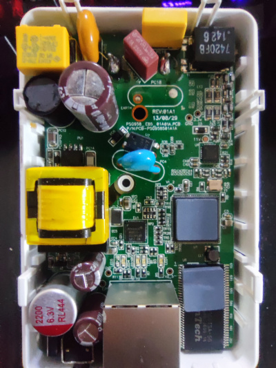
|
TrendNet TPL-408E2K/UK - 2015 Trend's TPL-480E series of powerline network adapters, seen here as the E2K variant, implemented the HomePlug AV2 standard, but this unit was extremely first generation. The advertised "600 Mbps" caused massive consumer confusion! This was the raw PHY (physical layer) rate, after demodulation the MAC (media access control) data rate was 200 Mbps, which these adapters come very close to. As a first generation AV2 implementation (based on Atheros' AR1540 + AR8035A) the PHY ran at 600 Mbps (maximum), and user data around 200 Mbps, similar to HomePlug AV, as extended by Atheros. The underlying technology is based on IEEE-1901 and belongs to the ITU-T's series of recommendations, as G.hn (G.9960, G.9961) in this case. The interoperability (co-existence) recommendation is G.9972. The physical data layer is very similar to VDSL. The next generation of devices extended speeds even more, using multiple spatial streams, to a raw PHY rate of 1.3 Gbps, resulting in a MAC rate of 550 Mbps. The use of HomePlugs could be prosecuted the UK under the Wireless Telegraphy Act, as they broadcast on licenced channels, using bands from 2 MHz to 30 MHz (Atheros extended this from 30 to 63 MHz). AV2 can additionally go as high as 83 MHz. A successful prosecution would require the operator to be causing interference to official communications (so a licenced user), and to have refused to cease such interference. As they're given out by major ISPs (including BT), it would be a quite ballsy move to try prosecuting under the Wireless Telegraphy Act. The power output is 24 dBm, or 0.25 watts, which is more than enough to interfere with shortwave radios, such as amateur radio and CB, over a several kilometer distance. Home wiring, being unshielded, long, with numerous straight runs of different lengths is surprisingly effective as an antenna! Trend's "Power Packet" utility (mirrored here, version 7.1.15) is a GUI atop of WinPCap and gives options for things like VLAN tagging and encryption setup. Default encryption settings are not secure and can be sniffed on by neighbours or attackers on the same circuit from quite some distance. Don't bother hunting for new firmware, version 5.3.5317 is the latest (and only) version widely known. Inside is a fairly simple setup, the AR1540 HomePlug AV2 controller with AR8035A gigabit ethernet transceiver (PHY), Etrontech SDRAM, a Cosmo 1010 optoisolator and a small SMPS, made up of mains capacitor, inductor, transformer and Power Integrations' TNY284DG SMPS controller. I haven't reverse engineered the SMPS layout, but it seems like a simple LC tank. After buying Atheros, Qualcomm renamed the AR1540 to the QCA7450. Atheros, like with most of its microcontroller-requiring products, used an ARM11 core to run the system. The later QCA7500 introduced MIMO capability, which was sort of the point of HomePlug AV2 over HomePlug AV! This unit went into use in an almost ideal case. Networking was at one side of a room, work laptop at the other, and WiFi had an issue which I didn't have time to properly investigate (later shown to be a very badly behaving Netgear WAC-124). While both TPL-408E2Ks were on power strips, they ultimately went to the same double mains socket, so an absolutely ideal use case for them. They hovered between 180 and 195 Mbps which was also almost ideal. |
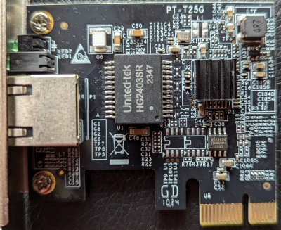
|
Realtek Gaming 2.5 GbE - 2015 Such a cute little NIC! Under the heatsink is a tiny Realtek 2.5 GbE MAC/PHY which identifies as device 8125, so is probably the RTL8125. Removing the heatsink off such a small BGA chip would possibly rip the chip off the PCB, so this wasn't done. The PCB is silkscreened "PT-T25G" and there are only four major components. A small 8 pin Winbond W25X40CL is a 4 Mbit flash memory with a serial interface, likely holding the NIC's bootstrap firmware, the large United-tek HG2403SR is the isolation transformer, and the top right of the card has the tell-tale capacitors, inductor (4.7 microHenrys), and MOSFET beneath of a voltage regulator module. One might wonder whether the 2.5 Gbit would be bottlenecked by the PCIe x1 interface. Single lane bandwidth on PCIe is 250 MB (decimal MBs) per second on PCIe 1.0, doubling to 500 MB/s in PCIe 2.0 and almost-doubling to 985 MB/s in PCIe 3.0. Real transfer rates are a bit weird, since a 8b/10b (PCIe 1.0, 2.0) or 128b/130b (3.0 - 5.0) binary code is used, so a PCIe 1.0/2.0 loses 20% of possible bandwidth to encoding overhead, while PCIe 3.0-5.0 lose less than 2%. Anyway, the interface here is PCIe 3.0 and the per-lane bandwidth is 8 Gbps, far more than the 2.5 Gbps this NIC is able to achieve. This NIC was brought in to replace a Realtek RTL8168 which was on the server's motherboard. RTL8167/68/69 cannot do jumbo frames properly and the network was starting to throw a lot of traffic around, causing high CPU use. This was also in the early stages of converting the core network to 2.5 GbE, so while a 1 GbE NIC would have been almost free, it made sense to go with 2.5 GbE. |
 Hattix hardware images are licensed under a Creative Commons Attribution 2.0 UK: England & Wales License except where otherwise stated.